Theoretically, signals in the fast clock domain will always sample signals transmitted from the slow clock domain. If the clocks are asynchronous, sampling errors may occur, so synchronization is required. This type of synchronization is relatively simple and generally uses the delay tapping method or the delayed sampling method.
Delay Tapping Method
The most common synchronization method is the two-stage flip-flop buffering method, commonly known as the delay tapping method. Before an asynchronous signal enters another clock domain, the signal is buffered twice consecutively by two stages of flip-flops, which effectively reduces metastability problems caused by timing violations. The circuit diagram is shown below.
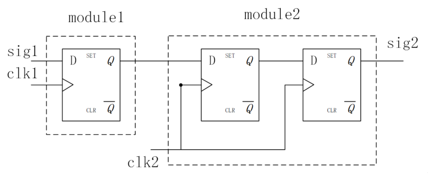
In general designs, using two stages of flip-flops for buffering is sufficient to meet design timing requirements. A large number of experiments show that three-stage flip-flop buffering can solve more than 99% of such asynchronous timing problems.
The Verilog description of two-stage flip-flop delay tapping and rising-edge detection is as follows:
Example
input clk1, // Asynchronous slow clock
input sig1, // Asynchronous signal
input rstn, // Reset signal
input clk2, // Destination fast clock domain clock
output sig2); // Signal synchronized in the fast clock domain
reg [2:0] sig2_r ; // 3-stage buffer; first two stages for synchronization, last two stages for edge detection
always @(posedge clk2 or negedge rstn) begin
if (!rstn) sig2_r <= 3'b0 ;
else sig2_r <= {sig2_r[1:0], sig1} ; // Buffer
end
assign sig2 = sig2_r[1] && !sig2_r[2] ; // Rising edge detection
Delayed Sampling Method
This method is mainly aimed at multi-bit data transmission.
For example, when the frequency ratio of two asynchronous clocks is 5, you can first use the delay tapping method to buffer the data enable signal through two stages of registers, and then sample the data signal from the slow clock domain in the fast clock domain.
The basic idea of this method is to ensure that the signal is safely sampled at the right moment, without needing to synchronize multi-bit data signals, thus saving some hardware resources.
The Verilog description of delayed sampling using the tapping method is as follows.
Example
// Asynchronous data comes from a module with a 20MHz working clock
module delay_sample(
input rstn,
input clk1,
input [31:0] din,
input din_en,
input clk2,
output [31:0] dout,
output dout_en);
//sync din_en
reg [2:0] din_en_r ;
always @(posedge clk2 or negedge rstn) begin
if (!rstn) din_en_r <= 3'b0 ;
else din_en_r <= {din_en_r[1:0], din_en} ;
end
wire din_en_pos = din_en_r[1] && !din_en_r[2] ;
//sync data
reg [31:0] dout_r ;
reg dout_en_r ;
always @(posedge clk2 or negedge rstn) begin
if (!rstn)
dout_r <= 'b0 ;
else if (din_en_pos)
dout_r <= din ;
end
//dout_en delay
always @(posedge clk2 or negedge rstn) begin
if (!rstn) dout_en_r <= 1'b0 ;
else dout_en_r <= din_en_pos ;
end
assign dout = dout_r ;
assign dout_en = dout_en_r ;
endmodule
The timing result diagram of this method is shown below.
Obviously, in the clk2 clock domain, sampling and buffering data at time t2 is much safer than at time t1.
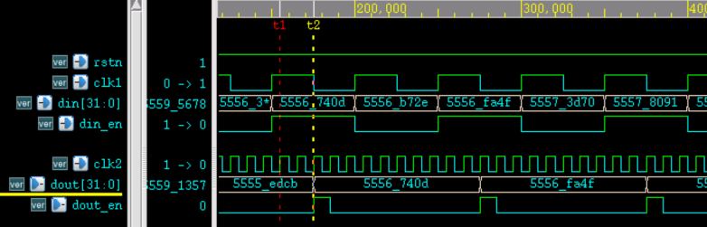
However, if the slow clock domain has no data enable signal din_en, or the data enable signal is always active, the method of detecting the rising edge of the data enable signal in the fast clock domain will fail. Because the data enable signal is always active, except for the first data, the fast clock domain will not be able to detect the transmission times of subsequent data.
The solution is to detect the edge of the slow clock signal in the fast clock domain.
If the frequency difference between the two clocks is small, it may be necessary to delay-buffer the data to ensure that the sampled data corresponds to the current clock beat; if the frequency difference is large, the data sampling time can be obtained by counting, without buffering the data.
The Verilog description of detecting the slow clock edge by using the counting delayed sampling method is as follows.
Example
// Asynchronous data comes from a module with a 999KHz working clock
module delay_cnt_sample(
input rstn,
input clk1,
input [31:0] din,
input din_en,
input clk2,
output [31:0] dout,
output dout_en);
// 4-stage buffer: 3 stages for tapping synchronization, 1 stage for edge detection
reg [3:0] edge_r ;
always @(posedge clk2 or negedge rstn) begin
if (!rstn) edge_r <= 3'b0 ;
else edge_r <= {edge_r[3:0], clk1} ;
end
wire edge_pos = edge_r[2] && !edge_r[3] ;
// Delay counter: starts counting when the slow clock rising edge is detected
reg [5:0] cnt ;
always @(posedge clk2 or negedge rstn) begin
if (!rstn) cnt <= 6'h3f ;
else if (edge_pos && din_en)
cnt <= 6'h0 ;
else if (cnt != 6'h3f) cnt <= cnt + 1'b1 ;
end
// Data synchronization
reg [31:0] dout_r ;
reg dout_en_r ;
always @(posedge clk2 or negedge rstn) begin
if (!rstn)
dout_r <= 'b0 ;
else if (din_en && cnt == 47) // Sample approximately at the middle of the slow clock period
dout_r <= din ;
end
// The data enable signal is output one cycle delayed from the data sampling time
always @(posedge clk2 or negedge rstn) begin
if (!rstn) dout_en_r <= 1'b0 ;
else if (din_en && cnt==48)
dout_en_r <= 1'b1 ;
else dout_en_r <= 1'b0 ;
end
assign dout = dout_r ;
assign dout_en = dout_en_r ;
endmodule
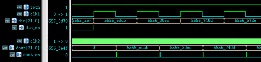
The data synchronization sampling result diagram for a large frequency difference is shown below.
As can be seen from the figure, the fast clock sampling time is around the center of the slow clock period, which is very safe.
Source Code Download for This Chapter
Download