NAND gate example
In a combinational logic UDP, the state table specifies different input combinations and corresponding output values. Any unspecified combination outputs x.
A simple NAND gate UDP can be expressed as follows:
output out ;
input a, b ;
table
//a b : out ;
0 0 : 1 ;
0 1 : 1 ;
1 0 : 1 ;
1 1 : 0 ;
endtable
endprimitive
As explained in the previous section, the port list and declaration section can be changed to:
output out,
input a, b);
......
endprimitive
State table items
The syntax format for each row in the state table representing combinational logic is as follows:
<input1> <input2> ... <inputN> : <output> ;
- 1. The order of the input signals in the state table must be consistent with the order of the UDP port list.
- 2. Input and output use a colon:to separate them.
- 3. Each row of the state table ends with a semicolon;to end.
- 4. All input combinations that can produce a definite output value must be listed in the state table, otherwise an x value will be output.
For example, in the above UDP nand_my, if a=0, b=x, then the output out = x, because this combination cannot be found in the table. Therefore, when writing a UDP, all input combinations must be fully considered.
The state table of UDP nand_my can be modified to:
//a b : out ;
0 0 : 1 ;
0 1 : 1 ;
1 0 : 1 ;
1 1 : 0 ;
0 x : 1 ;
x 0 : 1 ;
endtable
Don't care terms
In UDP nand_my, when either a or b is 0, the output is 1.
Input signals that do not affect the output result are don't care terms, which can be represented by a question mark "?". The "?" item in the state table will be automatically expanded to 0, 1, or x.
Therefore, the state table of UDP nand_my can be changed to:
//a b : out ;
0 ? : 1 ;
? 0 : 1 ;
1 1 : 0 ;
// The following combination will output x, so it can also be omitted. Verilog defaults to output x.
1 x : x ;
x 1 : x ;
endtable
UDP instantiation
The UDP invocation format is exactly the same as the built-in gate-level primitives.
Use the above UDP nand_my to complete"1.3 Gate Delay"simulation of the D flip-flop in.
With the delay information removed, the D flip-flop model is as follows.
Examples
input D, CP,
output Q, QR);
//part1, not gate
wire CPN, DN ;
not (CPN, CP);
not (DN, D);
//part2, master trigger
wire G3O, G4O ;
nand_my (G3O, D, CP);
nand_my (G4O, DN, CP);
wire G1O, G2O ;
nand_my (G1O, G3O, G2O);
nand_my (G2O, G4O, G1O);
//part3, slave trigger
wire G7O, G8O ;
nand_my (G7O, G1O, CPN);
nand_my (G8O, G2O, CPN);
wire G5O, G6O ;
nand_my (G5O, G7O, G6O);
nand_my (G6O, G8O, G5O);
assign Q = G5O ;
assign QR = G6O ;
endmodule
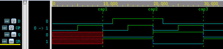
The testbench remains unchanged, and the simulation results are as follows.
As can be seen from the figure, the flip-flop captures the D input signal on the falling edge of the clock CP and passes it to Q/QR, which remains unchanged within a single clock cycle.
The NAND gate implemented by the UDP functions correctly.
Source code download for this chapter
Download