Keywords: gate delay, D flip-flop
Gate delay types
The gate-level circuits introduced in the previous two sections have no delay; actual gate-level circuits all have delay.
Verilog allows users to specify gate delays to define the propagation delay from inputs to output signals.
There are mainly three types of gate delays.
Rise delay
When a gate input changes, the transition time required for the gate output to change from 0, x, z to 1 is called the rise delay.
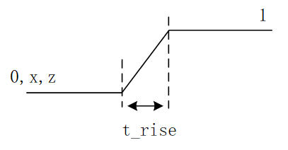
Fall delay
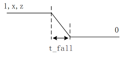
When a gate input changes, the transition time required for the gate output to change from 1, x, z to 0 is called the fall delay.
Turn-off delay
Turn-off delay refers to the transition time required for the gate output to change from 0, 1, x to the high-impedance state z.
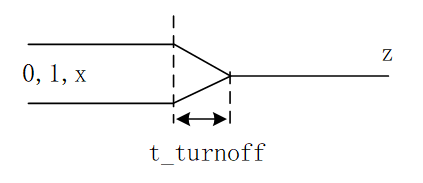
The transition time required for a gate output to change from 0, 1, z to x is not explicitly defined, but the time required can be determined by the other delay types; it is the smallest of the above three delay values.
Gate delays can be defined when instantiating a gate primitive. The definition format is as follows:
gate_type [delay] [instance_name] (signal_list) ;
Here, the number of delays can be 0, 1, 2, or 3.
The following table shows the delay values for different numbers of delay specifications.
| Delay type | No delay | 1 delay (d) | 2 delays (d1, d2) | 3 delays (d1, d2, d3) |
|---|---|---|---|---|
| Rise | 0 | d | d1 | d1 |
| Fall | 0 | d | d2 | d2 |
| Turn-off | 0 | d | min(d1, d2) | d3 |
| to_x | 0 | d | min(d1, d2) | min(d1, d2, d3) |
If no delay value is specified, the default delay is 0.
If the user specifies 1 delay value, then all types of delay values are equal to that value.
If the user specifies 2 delay values, they represent the rise delay and fall delay respectively, and the turn-off and "to_x" delays are both the smaller of these 2 delay values.
If the user specifies 3 delay values, they represent the rise delay, fall delay, and turn-off delay respectively, and the "to_x" delay is the smallest of these 3 delay values.
A gate-level primitive instantiation with delay values is as follows:
Example
and #(1) (OUT1, IN1, IN2) ;
//rise delay = 2.1, fall dalay = 2, trun-off delay = 2
or #(2.1, 2) (OUT2, IN1, IN2) ;
//rise delay = 2, fall dalay = 1, trun-off delay = 1.3
bufif0 #(2, 1, 1.3) (OUT3, IN1, CTRL) ;
It should be noted that multi-input gates (such as AND gates) and multi-output gates (such as NOT gates) can only define at most 2 delays, because the output will not be z.
Three-state gates and unidirectional switches (MOS transistors, CMOS transistors, etc.) can define 3 delays.
Pull-up and pull-down gates do not have any delay, because they represent a hardware attribute; the pull-up/pull-down state does not change and there is no output value.
Bidirectional switches (tran) have no delay when transmitting signals, and delay definitions are not allowed.
Bidirectional switches with control terminals (tranif1, tranif0) have a turn-on or turn-off delay when switching. Such bidirectional switches can be specified with 0, 1, or 2 delays, for example:
Example
tranif0 #(1) (inout1, inout2, CTRL);
//turn-on delay = 1, turn-off delay = 1.2
tranif1 #(1, 1.2) (inout3, inout4, CTRL);
Minimum/typical/maximum delays
Due to differences in integrated circuit manufacturing processes, the delay of devices in actual circuits always fluctuates within a certain range. In Verilog, users can not only specify the 3 types of gate delays, but also specify the minimum, typical, and maximum values for each type. At the compilation or simulation stage, one of these delay values can be selected, providing support for more realistic simulation.
- Minimum value: the minimum delay that the gate primitive has.
- Typical value: the typical delay that the gate primitive has.
- Maximum value: the maximum delay that the gate primitive has.
The following instantiation example illustrates the use of minimum, typical, and maximum delays.
Example
and #(1:2:3) (OUT1, IN1, IN2) ;
//rise delay: min 1, typical 2, max 3
//fall delay: min 3, typical 4, max 5
//turn-off delay: min min(1,3), typical min(2,4), max min(3,5)
or #(1:2:3, 3:4:5) (OUT2, IN1, IN2) ;
//rise delay: min 1, typical 2, max 3
//fall delay: min 3, typical 4, max 5
//turn-off delay: min 2, typical 3, max 4
bufif0 #(1:2:3, 3:4:5, 2:3:4) (OUT3, IN1, CTRL) ;
D flip-flop
Next, we design a D flip-flop from the perspective of gate-level modeling.
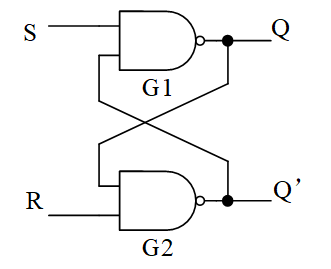
SR flip-flop
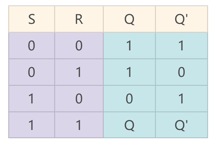
The SR flip-flop structure diagram and truth table are as follows.
- 1. When S is low, the output Q of G1 is high and is fed back to the input of G2. If R is high at this time, the output Q' of G2 is low.
- 2. When R is low and S is high, the analysis is similar.
- 3. When both S and R are high, if Q = 1 (Q' = 0), then after Q is fed back to the input of G2, the output Q' remains 0; after Q' is fed back to the input of G1, the output Q remains 1, showing a steady state. If Q = 0 (Q' = 1), the analysis is similar, and Q and Q' remain unchanged. That is, when both S and R are high, the circuit has a hold function.
- 4. If both S and R are low, then outputs Q and Q' are both high, and they are no longer complementary. Therefore, this case is forbidden.
SR latch
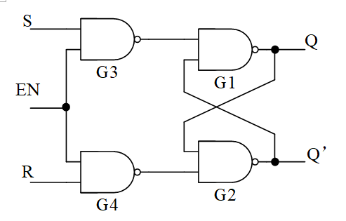
Adding two NAND gates in front of the basic SR flip-flop forms an SR latch with an enable terminal.
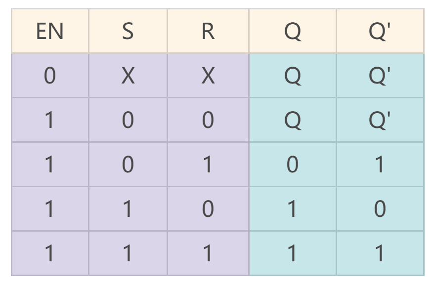
The SR latch and its truth table are as follows.
- When EN=0, G3 and G4 are disabled, and the SR latch holds its output state unchanged.
- When EN=1, it works exactly the same as the basic SR flip-flop.
D latch
The inputs of the basic SR flip-flop cannot both be 0, and the inputs of the SR latch with an enable terminal cannot both be 1; otherwise, it causes the non-complementary contradiction between outputs Q and Q'.
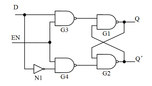
To eliminate this forbidden state, an inverting module is added to the SR latch with an enable terminal, ensuring that the 2 inputs are always opposite in logic, thus forming a D latch.
Its structure diagram and truth table are as follows.
- 1. When EN=1, the output state changes with the input state.
- 2. When EN=0, the output state remains unchanged.
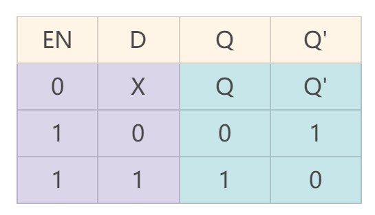
A D latch is level-triggered.
If the D input signal toggles multiple times during the active period of EN=1, the output Q will also toggle multiple times. This reduces the circuit's noise immunity and is not a safe circuit for practical requirements.
To improve the reliability of the flip-flop and enhance the circuit's noise immunity, the D flip-flop, which latches the signal at a specific moment, was invented.
D flip-flop
Cascading two D latches with the clock inverted forms a simple D flip-flop, also known as a Flip-flop.
Its structure diagram and truth table are as follows.
The first-stage D latch is also called the master latch, which latches when CP is low. The second-stage D latch is also called the slave latch; its clock is opposite to that of the master latch, and it latches when CP is high.
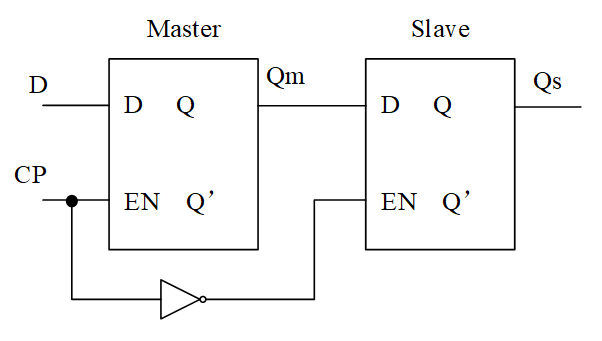
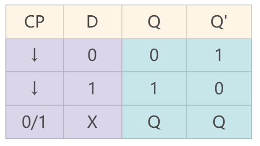
- 1. When CP=1, the master latch output Qm follows the changes of the D input signal, while the slave latch is in the hold state and its output Qs remains unchanged.
- 2. When CP changes from high to low, the master latch latches the current D state, transfers it to output Qm, and keeps it unchanged. The slave latch output Qs follows the changes of Qm. At this time, the master latch in the latched state keeps Qm unchanged, so after the D flip-flop output Qs receives the new Qm value, it also remains unchanged.
In summary, the D flip-flop output Qs latches the signal at D only on the falling edge of the clock CP; at other times, the output signal has a hold function.
Expanding the two-stage D latch into a gate-level structure is shown in the following figure.
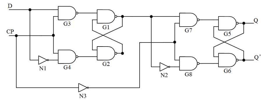
We perform gate-level modeling of the D flip-flop and add gate-level delays. The Verilog model is as follows:
Example
input D, CP,
output Q, QR);
parameter RISE_TIME = 0.11 ;
parameter FALL_TIME = 0.07 ;
//part1, not gate
wire CPN, DN ;
not #(RISE_TIME, FALL_TIME) (CPN, CP);
not #(RISE_TIME, FALL_TIME) (DN, D);
//part2, master trigger
wire G3O, G4O ;
nand #(RISE_TIME, FALL_TIME) (G3O, D, CP);
nand #(RISE_TIME, FALL_TIME) (G4O, DN, CP);
wire #(RISE_TIME, FALL_TIME) G1O, G2O ;
nand #(RISE_TIME, FALL_TIME) (G1O, G3O, G2O);
nand #(RISE_TIME, FALL_TIME) (G2O, G4O, G1O);
//part3, slave trigger
wire G7O, G8O ;
nand #(RISE_TIME, FALL_TIME) (G7O, G1O, CPN);
nand #(RISE_TIME, FALL_TIME) (G8O, G2O, CPN);
wire G5O, G6O ;
nand #(RISE_TIME, FALL_TIME) (G5O, G7O, G6O);
nand #(RISE_TIME, FALL_TIME) (G6O, G8O, G5O);
assign Q = G5O ;
assign QR = G6O ;
endmodule
The testbench is written as follows:
Example
module test ;
reg D, CP = 0 ;
wire Q, QR ;
always #5 CP = ~CP ;
initial begin
D = 0 ;
#12 D = 1 ;
#10 D = 0 ;
#14 D = 1 ;
#3 D = 0 ;
#18 D = 0 ;
end
D_TRI u_d_trigger(
.D (D),
.CP (CP),
.Q (Q),
.QR (QR));
initial begin
forever begin
#100;
//$display("---gyc---%d", $time);
if ($time >= 1000) begin
$finish ;
end
end
end
endmodule // test
The simulation results are as follows.
As can be seen from the figure, both Q/QR signals capture the D signal on the falling edge of the clock CP, remain unchanged within a single cycle, and the output has a delay.

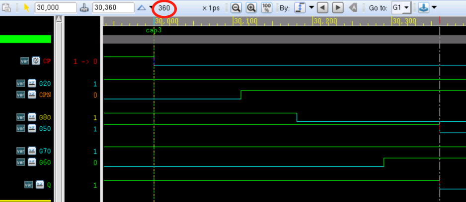
Enlarge the cap3 moment and trace the delay, as shown in the figure below.
- There is a rising delay from CP to CPN of 110ps;
- There is a falling delay from CPN to G8O of 70ps;
- There is a rising delay from G8O to G6O of 110ps;
- There is a falling delay from G6O to Q of 70ps;
- The total is 360ps, which matches the configured gate delay.
Download source code for this chapter
Download